Interesting Tech Projects
Tenting Vias in DesignSpark PCB
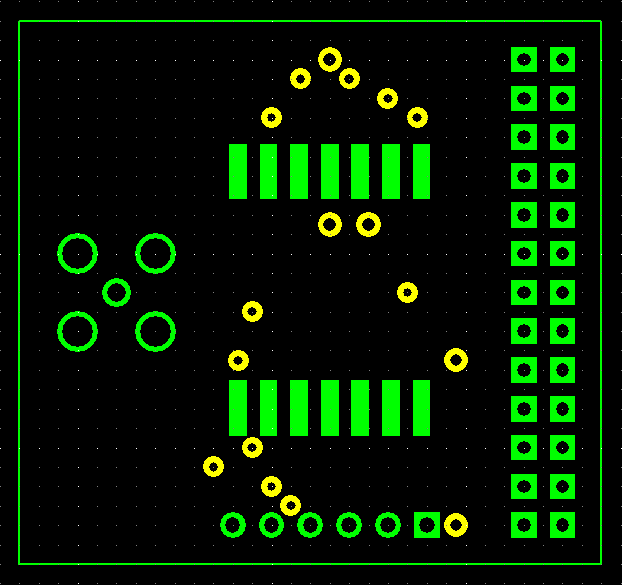
Sometimes it is useful to cover vias with solder mask. Here is how to do it in DesignSpark PCB. First the solder mask with the vias exposed:
1. Choose Design Technology… from the Settings menu
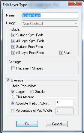
2. Click on the Solder Mask row and then the Edit… button
3. Uncheck the Vias setting and click on OK.
4. Click on OK to close the dialog window.
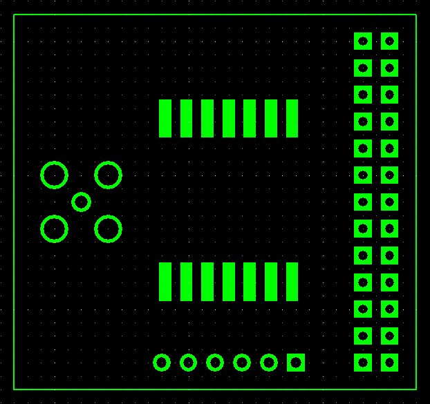
At this point the solder mask should automatically update to show the vias are now covered. If it doesn’t deselect the layer and reselect it to force a refresh.
| Print article | This entry was posted by Andy on October 10, 2014 at 3:20 pm, and is filed under Computer Aided Design, Electronics. Follow any responses to this post through RSS 2.0. Both comments and pings are currently closed. |
Comments are closed.


about 6 years ago
This is exactly what I’m looking for. Great! Thank you.
about 6 years ago
But it seems that this setting has no effect to the Manufacturing Plots (Gerber). Vias are uncovered. (DS PCB 8.0) 🙁
about 6 years ago
Perhaps send a bug report to RS? I’ve now switched to KiCAD – I think it’s significantly better than DesignSpark, as well as being free.
about 6 years ago
Very many thanks for this tip.
Works just fine on DS PCB 8.1